Vacuum table
These days, the needs of customer for processing the thin substrate
by using the PCB prototyping machine increases.
It is suitable to use vacuum table when processing on the thin
substrate materials.
Two models of the vacuum tables
MITS handles two kinds of vacuum tables. Please choose one in
accordance with
your purpose.
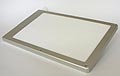
Popular model VT-ABS
Popular vacuum table made of the porous plastic resin. Compliant
with the substrate board thicker than 200µm
|
 |
| Items |
VT-ABS |
| Working area W x D (mm) |
300 x 170 / 229 x 295 |
| The thinnest substrate thickness (µm) |
200 |
| Material of the porous surface |
Plastic resin |
| Vulnerability |
Strong |
| Price |
Affordable |
| Compliant model |
FP-21T, FPZ-31AT
/ Eleven Lab, Auto Lab |
|
The principle of
the vacuum table and its advantage
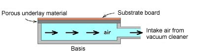
The fundamental principle is shown above.
The advantage is to aspirate the substrate very firmly, instead
of fixing them by
Scotch tape.
Material and the surface flatness
The crucial factor in choosing the vacuum table is the thickness
of the substrate board.
In case of processing the thin substrate board, you need to choose
the vacuum
table whose surface flatness is sufficient. If the surface flatness
is bad, it causes
uneven width of the track or penetration of the tools into the
substrate board.
In case that the end mill penetrates
the substrate, the vacuum table
will not be able to function
When the surface of the porous table gets damaged, the aspiration
performance and the flatness become deteriorate. Therefore, in
processing the substrate, we recommend that you should avoid drilling
and routing and that you should perform the milling not to penetrate
the substrate.
|
Fine Processing
MITS PCB prototyping machines are suitable not only for typical
PCB prototyping but also for fine processing of various types
of materials.
MITS
General Catalog
English
(PDF file / 1.8MB)
MITS Electronics
E-MAIL

Contact us : Inquiry Form
|