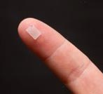
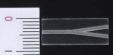
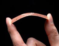
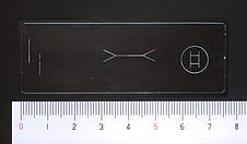
50µm(2mil) line and space, the state of the art! 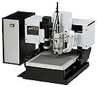 FP-21T Precision Stepping method and non-contacting pressure foot lead to the fine processing technology MITS General Catalog  English (PDF file / 1.8MB) MITS Electronics Contact us : Inquiry Form |
|||||||||||||||||||||||||||
50µm(2mil) line and space, the state of the art! FP-21T Precision Stepping method and non-contacting pressure foot lead to the fine processing technology MITS General Catalog English (PDF file / 1.8MB) MITS Electronics Contact us : Inquiry Form |
|||||||||||||||||||||||||||